The common emitter
In today’s post I would like to analyze the BJT common emitter amplifier configuration in depth. We will start from its simplest setup to the one that appears in the books, of course I will make some simulations to validate the theory.
The main motivation behind this post was me trying to understand how amplifiers work, why some weird approximations are made and more important what tools are needed to design one.
Setting the problem
Standard amplification consists of increasing the signal range to a constant factor, without modifying the signal in itself:
$$v_o(t) = A_v v_i(t) + V_{DC}$$
Ideally we want this kind of behaviour:
$$v_o(t) = A_v v_i(t)$$
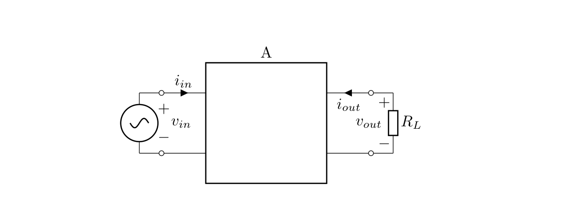
The amplifier we will be discussing requires a BJT transistor, which can be replaced by the models illustrated below:

They are known as the $\pi$-model (center diagram) and $\top$-model (right diagram), also remembering the following equations will be handy in the future.
$$ i_e = i_b + i_c $$ $$ i_c = \beta i_b $$ $$ i_e = \alpha i_c = (\beta + 1) i_b $$
$i_b$, $i_c$ and $i_e$ are base, collector and emitter currents respectively, and $\beta$ and $\alpha$ are intrinsic adimensional parameters of the transistor, $\beta$ is usually is specified in the device datasheet as $h_{FE}$.
Simplest setup
To implement the simplest common emitter amplifier we must check that the BJT transistor works in the active region. To do that first we have to bias a dc current through the base to ensure the transistor always conduct and second the collector must have a voltage supply able to handle the current gain required by the transistor otherwise the transistor will enter in cutoff mode (first rule broken) or saturation (second rule broken).
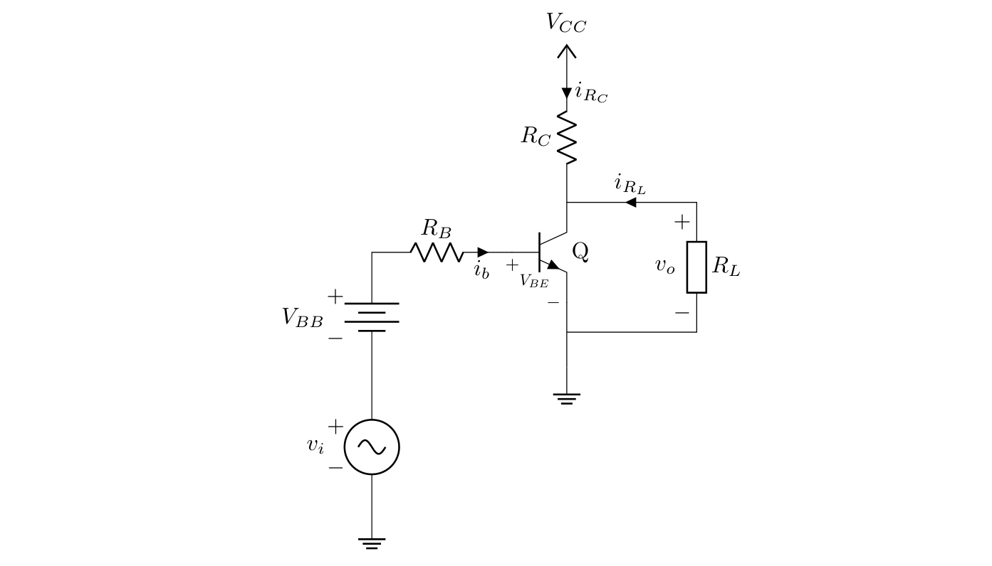
From the image above if we analyse the input loop we have that:
$$v_i + V_{BB} = i_b R_B + V_{BE}$$
Like diodes, a base to emitter voltage is generated when the transistor conducts, it usually is a value around 0.6 V.
Transistors are current amplifiers, so lets reorganize our formula to have $i_b$ in terms other variables:
$$ i_b = \frac{1}{R_B} \left( vi + V_{BB} - \underbrace{V_{BE}}_{0.6V}\right) > 0 $$
With the base current we can now analyse the output. Here is what you get if you look the loop from $V_{CC}$ through ground.
$$ V_{CC} = V_{RC} + \overbrace{v_{CE}}^{v_o} $$
$$ V_{CC} = R_C i_{RC} + v_{CE} $$
Now we need to express $i_{RC}$ in terms of the collector current $i_c$, to do that we know that $i_c$ is the sum of the currents flowing through $R_L$ and $R_C$, additionally the current through $R_L$ is equal to collector emitter voltage divided by the load $R_L$:
$$ i_c = i_{RC} + i_{RL} $$ $$ i_c = i_{RC} + \frac{-v_{CE}}{R_L} $$ $$ i_{RC} = i_c + \frac{v_{CE}}{R_L} $$
We can replace $i_{RC}$ and reorganize the formula to express $i_c$ in terms of $V_{CE}$:
$$ V_{CC} = R_C \overbrace{\left(i_c + \frac{v_{CE}}{R_L}\right)}^{i_{RC}} + v_{CE}$$
$$ i_c = \frac{V_{CC}}{R_C} - \left(\frac{1}{R_C} + \frac{1}{R_L}\right) v_{CE} $$
We know that $i_c = \beta i_b$, thus:
$$ \overbrace{\beta i_b}^{i_c} = \frac{V_{CC}}{R_C} - \left(\frac{1}{R_C} + \frac{1}{R_L}\right) v_{CE} $$
Bingo!, there is a way to relate the input with the output, we just have to replace $i_b$ using the formula found previously:
$$ \beta \overbrace{\frac{vi + V_{BB} - V_{BE}}{R_B}}^{i_b} = \frac{V_{CC}}{R_C} - \frac{R_L + R_C}{R_L R_C} v_{CE} $$
After some algebraic tweaks here is the output in terms of the input: $$ v_{CE} = v_o = \frac{R_L R_B V_{CC} + \beta R_C R_L ( V_{BE} - V_{BB}) }{R_B (R_L + R_C)} - \beta \frac{R_C}{R_B} \frac{R_L}{(R_L + R_C)} v_i $$
$$ v_o = V_{DC} - A v_i $$
This setup presents multiple issues:
- An unwanted DC component.
- The gain factor $\beta \frac{R_C}{R_B}$ depends of $\beta$, a property of the transistor which can not be controlled directly.
- The need of two sources to make the circuit work.
Before simulating the circuit and handling this issues lets discuss about the requirements needed to make the circuit work.
Avoiding Cutoff
As mentioned earlier, to prevent the transistor from turning off a current must be flowing through the base thus:
$$ i_b = \frac{1}{R_B} \left( v_{i} + V_{BB} - \underbrace{V_{BE}}_{0.6V}\right) > 0 $$
To guarantee the transistor is always conducting a proper $V_{BB}$ source must be selected using the minimal possible input voltage $\min (v_i)$:
$$ \frac{1}{R_B} \left( \min (v_i) + V_{BB} - \underbrace{V_{BE}}_{0.6V}\right) > 0 $$
$$ V_{BB} > V_{BE} - \min (v_i) $$
Preventing Saturation
To avoid this situation the power supply $V_{CC}$ must provide enough voltage to handle the current ($i_c$) required by the transistor. To find a proper $V_{CC}$ we need an equation which relates $i_c$ with $v_{CE}$:
$$ i_c = \frac{V_{CC}}{R_C} - \left(\frac{1}{R_C} + \frac{1}{R_L}\right) v_{CE} $$
Saturation happens when the transistor is conducting the maximum current it can ($\max (i_c)$), at this point $V_{CE}$ will converge asymptotically to 0 no matter how much current is applied to the transistor.
$$ \max (i_c) = \frac{V_{CC}}{R_C} - \left(\frac{1}{R_C} + \frac{1}{R_L}\right) {v_{CE}}_{(sat)} $$
$$ \beta \max (i_b) = \frac{V_{CC}}{R_C} - \left(\frac{1}{R_C} + \frac{1}{R_L}\right) {v_{CE}}_{(sat)} $$
Sometimes the data-sheet provider will give you a graph comparing the base or collector current against the collector-emitter voltage, like the one illustrated in the image below with a 2N2222A transistor, in this example the transistor enters in saturation when the line decreases at a slower rate until we get an almost horizontal line.
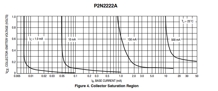
This diagrams can be used to determine the least $V_{CC}$ needed to avoid saturation, from the previous formula $i_b$ can be replaced by the following equation
$$ \beta \max(i_b) = \beta \frac{\max(v_i) + V_{BB} - V_{BE}}{R_B} $$
And $V_{CE(sat)}$ can be determined from the transistor’s data-sheet:
$$ \beta \frac{\max(v_i) + V_{BB} - V_{BE}}{R_B} = \frac{V_{CC}}{R_C} - \frac{R_L + R_C}{R_L R_C} {v_{CE}}_{(sat)} $$
After reorganizing we can now establish the minimum $V_{CC}$ to avoid saturation:
$$ \frac{V_{CC}}{R_C} \ge \beta \frac{\max(v_i) + V_{BB} - V_{BE}}{R_B} + \frac{R_L + R_C}{R_L R_C} {v_{CE}}_{(sat)} $$
$$ V_{CC} \ge \beta \frac{R_c}{R_b} ( \max(v_i) + V_{BB} - V_{BE} ) + \frac{R_L + R_C}{R_L} {v_{CE}}_{(sat)} $$
Simulating the Circuit
It is time to validate the theory with some simulations, for our circuit we will use the following components:
- 2N2222A transistor: $\beta \approx 180$, $V_{BE} \approx 0.6 V$, ${V_{CE}}_{(sat)} \approx 0.1V$ (here I used datasheet graphs instead of table values).
- $R_B$: $20k \Omega$
- $R_C$: $400 \Omega$
- $R_L$: $1k \Omega$
- $v_i$: $sin(2\pi 120 t)$
Now let’s find the necessary voltage values $V_{BB}$ and $V_{CC}$ to ensure the transistor stays in the active region.
- $V_{BB} \ge 0.7 - (- 1) V = 1.7 V$
- $V_{CC} \ge 180 \frac{400}{20k} ( 1.0 + \overbrace{2.0}^{V_{BB}} - 0.6 )V + \frac{1k + 400}{1k} 0.1 V \approx 8.78 $
“Rules are meant to be broken” one friend of mine said, so why not to break the constrains calculated before to see how circuit responses at cutoff, saturation and active operation:
- Cutoff:
- $V_{BB} = 1V$
- $V_{CC} = 10V$
- Saturation:
- $V_{BB}: 2V$
- $V_{CC}: 5V$
- Linear Behaviour:
- $V_{BB}: 2V$
- $V_{CC}: 10V$
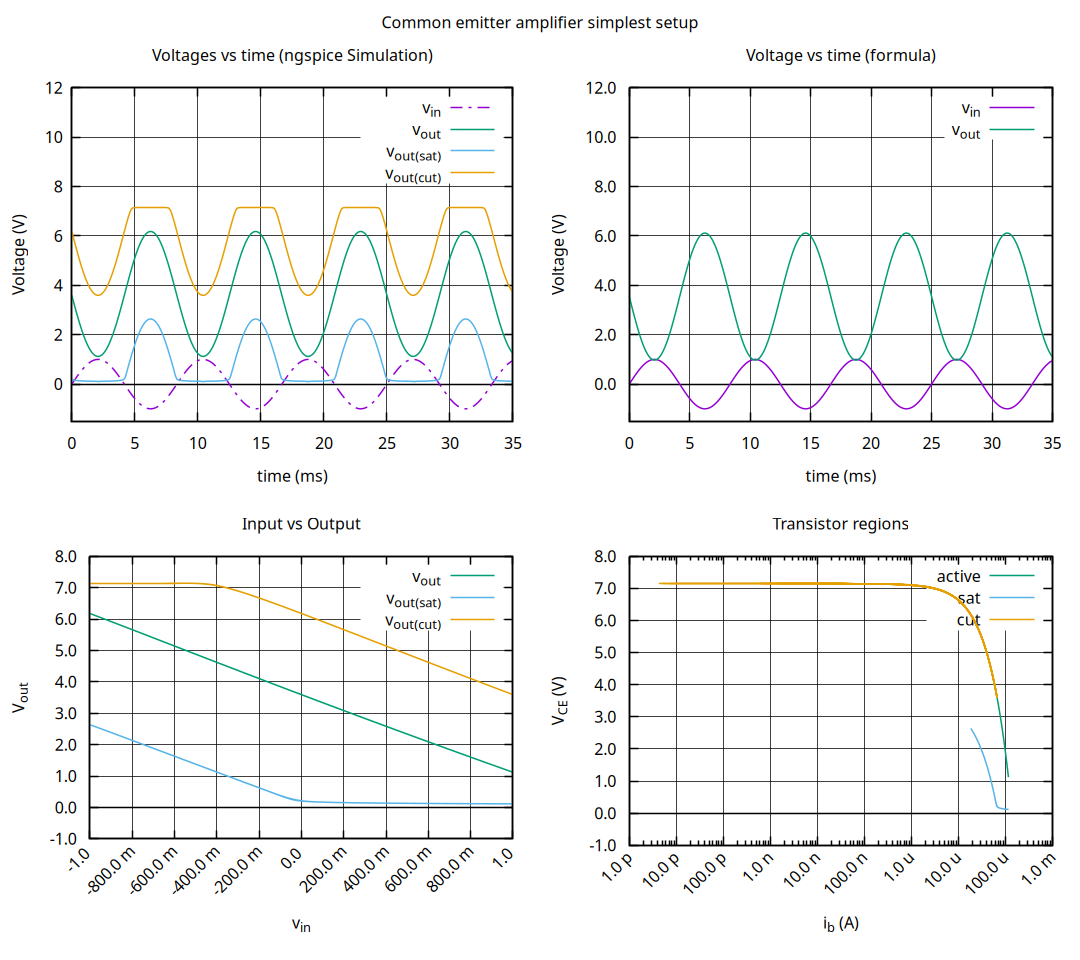
Formula vs simulation in active region results validate the theory, another observation to be made is the circuit response at saturation and cutoff, they seem counter-intuitive but you have to remember that the gain factor $- \beta \frac{R_C}{R_B} \frac{R_L}{R_L + R_C}$ inverts the input signal, the Transistor regions diagram illustrate quite well when the circuit enters in saturation or cutoff.
Removing the DC component.
As mentioned above the implementation illustrated presents some nasty inconveniences like a DC component at the output. Lets fix that problem putting a coupling capacitor at the output:
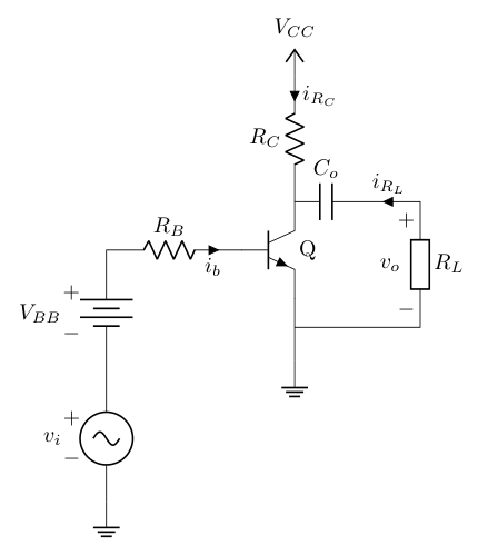
In conjunction with the load $R_L$, the capacitor will act as a high filter that can be adjusted to remove unnecessary low frequency components.
To calculate the gain we can use the same formula found previously:
$$ \beta \frac{vi + V_{BB} - V_{BE}}{R_B} = \frac{V_{CC}}{R_C} - \frac{R_L + R_C}{R_L R_C} v_{CE} $$
And replace $R_L$ for $Z_L$ where $Z_L$ to the impedance of $C_o$ in series with $R_L$. Because capacitance reacts at frequency components we will work with voltages and impedances in the frequency domain, making use of the Laplace transform, remember $s = \delta + j\omega$ where $\omega = 2 \pi f$.
$$ Z_L = \frac{1}{s C_o} + R_L = \frac{1 + s C_o R_L}{s C_o} $$
After replacing $R_L$ and reorganizing terms you should get something like this:
$$ \beta \frac{vi + V_{BB} - V_{BE}}{R_B} = \frac{V_{CC}}{R_C} - \left( \frac{1}{Z_L} + \frac{1}{R_C} \right) v_{CE} $$ $$ \beta \frac{vi + V_{BB} - V_{BE}}{R_B} = \frac{V_{CC}}{R_C} - \left( \frac{s C_o}{1 + s C_o R_L} + \frac{1}{R_C} \right) v_{CE} $$ $$ \beta \frac{vi + V_{BB} - V_{BE}}{R_B} = \frac{V_{CC}}{R_C} - \frac{s C_o R_C + 1 + s C_o R_L}{R_C + s C_o R_C R_L} v_{CE} $$ $$ \frac{s C_o (R_C + R_L) + 1}{R_C (1 + s C_o R_L)} v_{CE} = \frac{V_{CC}}{R_C} - \beta \frac{vi + V_{BB} - V_{BE}}{R_B} $$ $$ v_{CE} = \frac{1 + s C_o R_L}{s C_o (R_C + R_L) + 1} V_{CC} - \beta \frac{R_C (1 + s C_o R_L)}{s C_o (R_C + R_L) + 1} \frac{vi + V_{BB} - V_{BE}}{R_B} $$
$$ v_{CE} = \frac{R_B + s C_o R_B R_L}{s R_B C_o (R_C + R_L) + R_B} V_{CC} - \beta \frac{R_C (1 + s C_o R_L)}{s C_o R_B (R_C + R_L) + R_B} \left(vi + V_{BB} - V_{BE}\right) $$
$$ v_{CE} = \frac{(R_B + s C_o R_B R_L) V_{CC} + \beta (R_C + s C_o R_C R_L) (V_{BE} - V_{BB}) }{s R_B C_o (R_C + R_L) + R_B} - \beta \frac{R_C (1 + s C_o R_L)}{s C_o R_B (R_C + R_L) + R_B} v_i $$
Things are starting to get complicated, that’s why in other learning resources they make distinction between DC and AC analysis, where in DC capacitors are approximated as open circuits while in AC they are treated as shorts.
In the formula above we can distinguish two terms, one depending of DC voltage sources (signals with frequency 0) and another one depending of the input signal, which can be rewritten in the following way.
$$ v_{CE} = V_{DC} - A v_i $$
This time the output voltage $v_o$ is different from the voltage on the collector emitter voltage $v_{CE}$, to find out its value we just have to calculate a voltage divider between $v_o$ and $v_{CE}$:
$$ v_o = \frac{R_L}{Z_L} v_{CE} = \frac{s R_L C_o}{1 + s C_o R_L} v_{CE} $$
$$ v_o = \frac{s R_L C_o}{1 + s C_o R_L} (V_{DC} - A v_i) $$
$$ v_o = \overbrace{\frac{s R_L C_o }{1 + s C_o R_L} V_{DC}}^0 - A \frac{s R_L C_o }{1 + s C_o R_L} v_i $$
$\frac{s R_L C_o }{1 + s C_o R_L} V_{DC}$ can be removed from the equation due to the fact that $V_{DC}$ only exist at 0 frequency and the $s$ term multiplying $V_{DC}$ cancels out the hole term.
So here are the final equation after replacing $A$ term simplified previously.
$$ v_o = - \overbrace{\beta \frac{R_C (1 + s C_o R_L)}{s C_o R_B (R_C + R_L) + R_B}}^A \frac{s R_L C_o}{1 + s C_o R_L} v_i $$ $$ v_o(s) = - \frac{\beta R_C R_L }{R_B (R_C + R_L)} \frac{s}{s + \frac{1}{C_o (R_C + R_L)}} v_i (s) $$
In frequency domain it is better to use the transfer function, to understand how the circuit behaves no matter the input you apply.
$$ H(s) = \frac{v_o(s)}{v_i(s)} = - \frac{\beta R_C R_L }{R_B (R_C + R_L)} \frac{s}{s + \frac{1}{C_o (R_C + R_L)}} $$
$$ H(s) = - \beta \frac{ R_C}{R_B} \frac{R_L}{R_C + R_L} \frac{s}{s + \frac{1}{C_o (R_C + R_L)}} $$
The formula obtained resembles the one found in the previous setup, but without a DC component.
Lets simulate setting the output capacitor $C_o$ to $100 \mu F$ and using the same parameter values as before:
This time we will compare the simulation against the formula using Bode Plots.
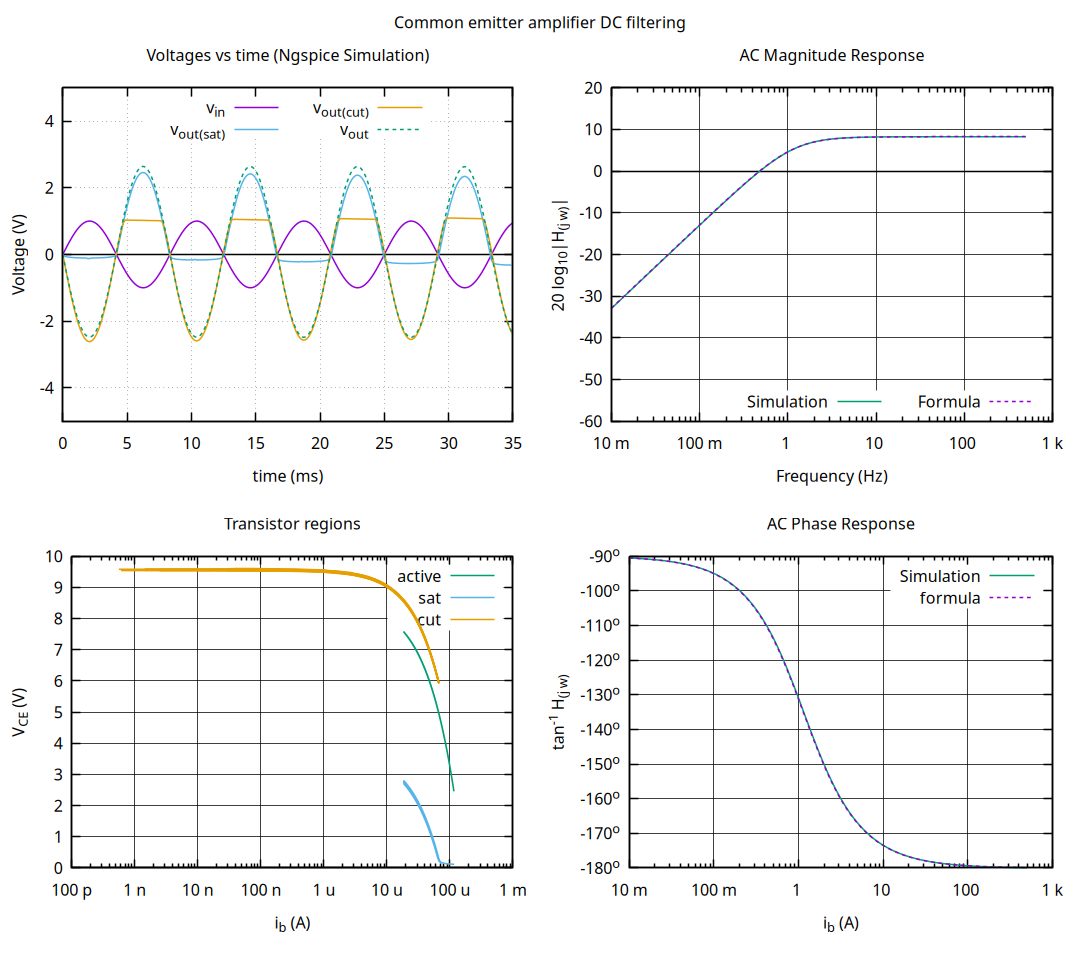
As you can see in the graph above, transistor regions are pretty similar to the first simulation, and if we compare the formula against the simulation in the Magnitude and Phase Bode Diagrams they seem identical which validates our assumptions.
A better way to bias the transistor
Having two sources to make a transistor work does not look like a practical idea, so why not to get rid of $V_{BB}$ source, and use $V_{CC}$ to bias the transistor.
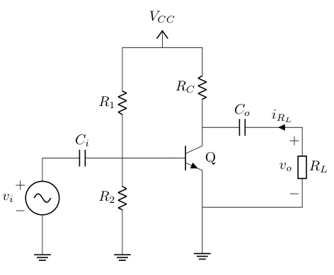
Well that seems better now we only rely in one DC source ($V_{CC}$) to amplify the input signal $v_i$, but there is problem that makes the circuit very susceptible to enter in saturation mode and it is the emitter connected to ground, to avoid this problem it is recommended to put a resistance through the emitter sufficiently large to ensure $1V$ at the emitter.
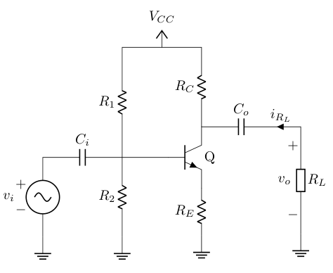
In contrast to other approaches where capacitors are replaced by shorts and open circuits for AC and DC analysis respectively we will go straight up analyzing the circuit in the frequency domain. The first thing we are going to do is to simplify the circuit at the input with the help of the Thévenin’s theorem.
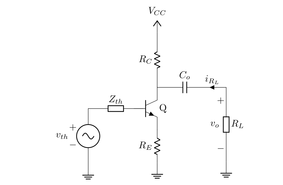
Here are the results of calculating $v_{th}$ an $Z_{th}$:
(1) $$ Z_{th} = \frac{R_1 R_2}{R_1 R_2 C_i s + R_1 + R_2} = \frac{1}{C_i}\frac{1}{s + \frac{R_1 + R_2}{C_i R_1 R_2}} $$ (2) $$ v_{th} = \overbrace{\frac{1}{C_i}\frac{1}{s + \frac{R_1 + R_2}{C_i R_1 R_2}}}^{Z_{th}} \left( \frac{1}{R_1} V_{CC} + s C_i v_i \right) $$
Here we can see the coupling action of the input capacitor, if you zoom out the equation we might recognize the formula presents the following pattern:
$$ v_{th} \approx \frac{1}{s + k} (s v_{AC} + V_{DC}) $$
Which correspond to the filtered input plus a DC component that ensures the transistor never enters in cutoff mode.
With Thévenin circuit simplification done it is time to replace the transistor for a linear model to get the circuit’s gain factor, we will use $\pi-model$, but I strongly recommend you to use $\top$-model to solve the circuit.
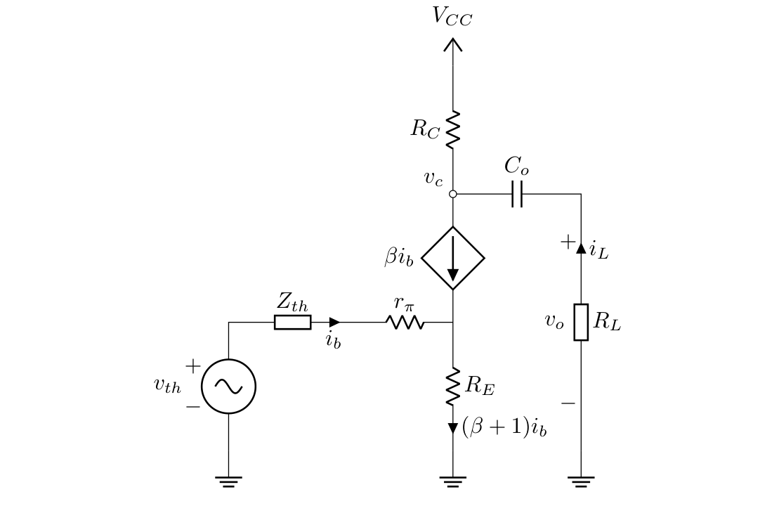
Lets calculate $v_c$ in terms of $v_o$ to use it later: $$ v_c = - \frac{1}{s C_o} i_L + v_o = \frac{1}{s C_o} \overbrace{\frac{v_o}{R_L}}^{- i_L} + v_o $$ $$ v_c = \left( 1 + \frac{1}{s C_o R_L} \right) v_o $$ $$ v_c = \frac{s C_o R_L + 1}{s C_o R_L} v_o $$
The current through the collector corresponds to the sum of the current load $i_L$ and the current passing through $R_C$:
$$ \overbrace{\frac{V_{CC} - v_c}{R_C}}^{i_{R_C}} + \overbrace{\frac{-v_o}{R_L}}^{i_L} = \beta i_b = i_c $$
Where $v_c$ can be replaced as follows: $$ \frac{V_{CC}}{R_C} - \frac{v_c}{R_C} - \frac{v_o}{R_L} = \beta i_b $$
$$ \frac{V_{CC}}{R_C} - \frac{1}{R_C} \overbrace{\frac{s C_o R_L + 1}{s C_o R_L} v_o}^{v_c} - \frac{v_o}{R_L} = \beta i_b $$
$$ \frac{V_{CC}}{R_C} - \frac{1}{R_C} \frac{s C_o R_L + 1 + s C_o R_C}{s C_o R_L} v_o = \beta i_b $$
We will reorganize the formula and annotate it:
(3) $$ \frac{V_{CC}}{R_C} - \frac{(R_L + R_C) C_o s + 1}{s R_C R_L C_o} v_o = \beta i_b $$
As before $i_b$ is the key to relate the input with the output, the expression above is a result of applying Kirchhoff laws at the output, to get $i_b$ in terms of the input we just need to checkout input loop to express $v_{th}$ in terms of $i_b$.
$$ v_{th} = ( Z_{th} + r_{\pi} ) i_b + (\beta + 1) R_E i_b $$
Which reorganized becomes in:
$$ i_b = \frac{1}{Z_{th} + r_{\pi} + (\beta + 1) R_E} v_{th} $$
Lets use (1) to have $i_b$ in terms of $v_i$: $$ i_b = \frac{Z_{th}}{Z_{th} + r_{\pi} + (\beta + 1) R_E} \left( \frac{1}{R_1} V_{CC} + s C_i v_i \right) $$
We now have everything to express $v_o$ in terms of $v_i$, we just need to replace $i_b$ on (3) reorganize its terms and we’re done.
$$ \frac{V_{CC}}{R_C} - \frac{(R_L + R_C) C_o s + 1}{s R_C R_L C_o} v_o = \beta \frac{Z_{th}}{Z_{th} + r_{\pi} + (\beta + 1) R_E} \left( \frac{1}{R_1} V_{CC} + s C_i v_i \right) $$
$$ \frac{(R_L + R_C) C_o s + 1}{s R_C R_L C_o} v_o = \frac{V_{CC}}{R_C} - \beta \frac{Z_{th}}{Z_{th} + r_{\pi} + (\beta + 1) R_E} \left( \frac{1}{R_1} V_{CC} + s C_i v_i \right) $$
$$ \frac{(R_L + R_C) C_o s + 1}{s R_C R_L C_o} v_o = \left( \frac{1}{R_C} - \frac{\beta Z_{th}}{R_1 (Z_{th} + r_{\pi} + (\beta + 1) R_E)} \right) V_{CC} - \frac{\beta Z_{th} C_i s}{Z_{th} + r_{\pi} + (\beta + 1) R_E} v_i $$ $$ v_o = \frac{s R_C R_L C_o}{(R_L + R_C) C_o s + 1} \left( \frac{R_1 r_{\pi} + (R_1 - \beta R_C) Z_{th} + R_1 (\beta + 1) R_E}{R_1 (r_{\pi} + Z_{th} + (\beta + 1) R_E)} V_{CC} - \frac{\beta Z_{th} C_i s}{r_{\pi} + Z_{th} + (\beta + 1) R_E} v_i \right) $$
From here we can make a little simplification taking advantage of the fact that every DC component will disappear at the output due to the $s$ factor, therefore the term multiplying $V_{CC}$ can be deleted.
$$ v_o = - \frac{s R_C R_L C_o}{(R_L + R_C) C_o s + 1} \frac{\beta Z_{th} C_i s}{r_{\pi} + Z_{th} + (\beta + 1) R_E} v_i $$
$$ v_o = - \frac{\beta R_C R_L}{R_L + R_C} \frac{s}{s + \frac{1}{(R_L + R_C) C_o}} \frac{Z_{th} C_i s}{r_{\pi} + Z_{th} + (\beta + 1) R_E} v_i $$
$r_{\pi}$ can be replaced by $(\beta + 1) r_e$ from $\top$-model, here the reason we encouraged you to use $\top$-model initially in our case we just mistakenly choose a more inconvenient path:
$$ v_o = - \frac{\beta R_C R_L}{R_L + R_C} \frac{s}{s + \frac{1}{(R_L + R_C) C_o}} \frac{Z_{th} C_i s}{Z_{th} + (\beta + 1) (r_e + R_E)} v_i $$
Finally to get the transfer function use (1) to replace $Z_L$, and practice your algebraic skills to get the following equation: $$ H(s) = \frac{v_o(s)}{v_i(s)} = - \frac{\beta}{\beta + 1} \frac{R_L}{R_L + R_C} \frac{R_C}{R_E + r_e} \frac{s}{s + \frac{1}{(R_L + R_C) C_o}} \frac{s}{s + \frac{1}{C_i (\beta + 1)(R_E + r_e)} + \frac{R_1 + R_2}{C_i R_1 R_2}} $$
There are multiple things to analyze in this circuit.
First lets take a look at $\frac{\beta}{\beta + 1}$, which is approximately equal to 1 and this is great because we no longer depend on $\beta$ to amplify the signal.
Second the term $\frac{R_C}{R_E + r_e}$, illustrates the importance of having a resistor connecting the emitter to ground, otherwise we would have to rely on $r_e$, which like $\beta$, can not be directly changed and is pretty susceptible to temperature changes, indeed this parameter is calculated as the thermic voltage (almost always is $25 \mu V$) over the $DC$ emitter current $\frac{V_T}{I_{e(DC)}}$.
Third the factor $\frac{R_L}{R_C + R_L}$ seems like a tensor divider, this term shows how the load decreases the maximum possible gain a circuit can provide, here is the reason why 1 gain amplifiers (or better called buffers) are needed.
Finally the terms $\frac{s}{s + \frac{1}{(R_L + R_C) C_o}}$ and $\frac{s}{s + \frac{1}{C_i (\beta + 1)(R_E + r_e)} + \frac{R_1 + R_2}{C_i R_1 R_2}}$ are filters that indicate at which frecuencies does the circuit operate.
Avoiding Saturation and Cutoff (again)
With the gain factor calculated, we now must find a proper setup to ensure the circuit is able to handle the gain provided by the transistor, otherwise we will find our circuit to be in saturation or cutoff region.
To do that we will get rid of the input and consequently its output and focus in the relationship between the collector to emitter voltage ($v_{CE}$) vs the base current ($i_b$) in the transistor at DC operation, this is the circuit we will be analyzing:
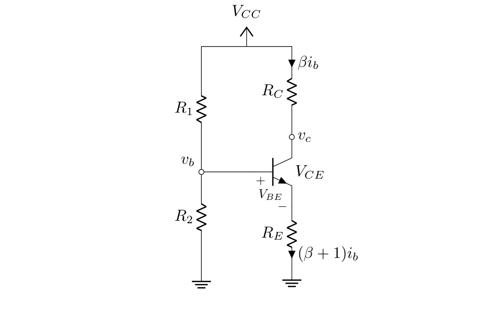
At DC this simplification is possible thanks to the coupling capacitors.
To get the relationship between $V_{CE}$ and $i_b$ we can use the fact that $V_{CC}$ is equal to the sum of voltages which pass through the transistor, $R_C$ and $R_E$ thus:
$$ V_{CC} = R_C \beta i_b + V_{CE} + R_E (\beta + 1) i_b $$
After reorganizing the formula we get the following expression:
(4) $$ V_{CE} = V_{CC} - ((R_C + R_E) \beta + R_E) i_b $$
From this formula we can extract the quiescent point of the transistor which is the point where the transistor can provide the greatest amplitude range without entering in saturation and cutoff regions.
First lets find the approximate maximum $V_{CE}$ voltage which corresponds to the point where $i_b$ is practically 0.
$$ V_{CE}(0) = V_{CC} $$
Now lets find the maximum current $i_b$ the transistor can receive which happens when $V_{CE}$ is close to 0:
$$ V_{CE} = 0 = V_{CC} - ((R_C + R_E) \beta + R_E) i_b $$
$$ i_b = \frac{V_{CC}}{(R_C + R_E) \beta + R_E} $$
We have two components of a triangle, the y component which corresponds to the transistor providing its maximum collector to emitter voltage, and the x component which corresponds to the transistor receiving its maximum base current, the quiescent point ($Q$) can be found easily dividing those component by 2.
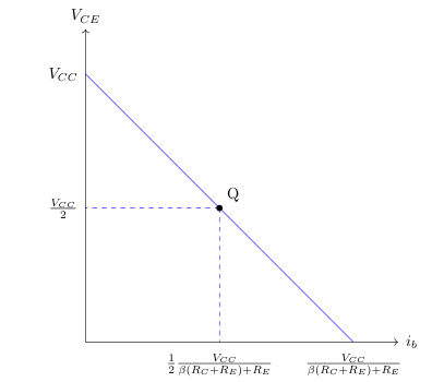
To design a common emitter amplifier we can take advantage of the x component to select $R_E$ and $R_C$.
First we have to reorganize our formula to get $R_C$ in terms of $i_{b(Q)}$.
$$ i_{b(Q)} = \frac{1}{2}\frac{V_{CC}}{(R_C + R_E) \beta + R_E} $$
$$ R_C = \frac{1}{2}\frac{V_{CC}}{\beta i_{b(Q)}} - R_E \left(1 + \frac{1}{\beta}\right) $$
In some cases it is handy to use $i_c$ instead of $i_b$:
$$ R_C = \frac{1}{2}\frac{V_{CC}}{i_{c(Q)}} - R_E \left(1 + \frac{1}{\beta}\right) $$
To determine $R_E$ choose a resistance that ensures at least $1 V$ at the emitter $V_E$, this is usually enough to guarantee thermal stability when the transistor is working in active region.
$$ V_E = \frac{i_{e(Q)}}{R_E} $$
$$ R_E = \frac{V_E}{i_{e(Q)}} = \frac{V_E}{(\beta + 1)i_{b(Q)}} = \frac{\beta}{\beta + 1} \frac{V_E}{i_{c(Q)}} $$
With $R_E$ and $R_C$ defined the other step is setting the ratio between $R_1$ and $R_2$, to achieve this goal we are going to focus on the input currents in the base node:
$$ \frac{V_{CC} - v_b}{R_1} - \frac{v_b}{R_2} = \frac{V_E}{(\beta + 1) R_E} = i_b $$
$V_{CC}$, $v_b$ and $V_E$ are values more or less in the same magnitude scale. If we make $\frac{1}{R_1} + \frac{1}{R_2}$ at least one order of magnitude (10) greater than $\frac{1}{(\beta + 1) R_E}$ we can approximate our previous formula to the following expression:
$$ \frac{V_{CC} - v_b}{R_1} - \frac{v_b}{R_2} \approx 0 $$
$$ \frac{R_2}{R_1} = \frac{v_b}{V_{CC} - v_b} $$
Remember this formula only works in cases when: $$ \frac{1}{R_1} + \frac{1}{R_2} > 10 \frac{1}{(\beta + 1) R_E} $$ or in other words:
$$ R_1||R_2 < \frac{1}{10} (\beta + 1) R_E $$
One thing to note here is that $(\beta + 1) R_E$ corresponds to the input resistance seen at the base.
The final simulation
Now we have all the tools to design and simulate a common emitter amplifier it is time to put them in practice.
Suppose we have an input signal coming from a sensor with a cut frequency of $500 Hz$ which varies from $-0.5 V$ to $0.5V$ that needs to be amplified to a voltage range starting from $-5V$ to $5V$. The output will be connected to a load $R_L = 10k\Omega$.
Lets redraw our common emitter amplifier:

To choose the proper resistances we need to establish the gain factor, therefore to pass from $0.5V$ to $-5V$ we need a gain of $20dB\angle{180}$ or -10:
$$ \frac{v_o}{v_i} = -\overbrace{\frac{\beta}{\beta + 1}}^{\approx 1} \frac{R_L}{R_L + R_C} \frac{R_C}{R_E + r_e} = -10 $$
Some approximations can be made to ease the process of getting the proper parameters values. $$ \frac{R_L}{R_L + R_C} \frac{R_C}{R_E} \approx 10 $$
Reorganizing the formula we will get: $$ R_C = \frac{10 R_L R_E}{R_L - 10 R_E} $$
Now we have one condition to get a proper $R_C$. The emitter resistance must be at most 10 times smaller than the load resistance $R_E < \frac{1}{10} R_L$, thus $R_E < 1k \Omega$.
Having in mind the condition above we can use the following formula fond $R_E$.
$$ R_E = \frac{\beta}{\beta + 1} \frac{V_E}{i_{c(Q)}} \approx \frac{V_E}{i_{c(Q)}} < 1k \Omega $$
Remember $V_E$ should be $1V$ and $i_{c(Q)}$ can be selected to fit your needs:
$$ R_E = \frac{1V}{2mA} = 500 \Omega $$
Now we have all we need to find $R_C$:
$$ R_C = \frac{10 \times 10k \times 500}{10k - 10 \times 500} = 10k \Omega $$
$R_C$ and $R_E$ were found, the collector current is defined, but how do we guarantee the transistor is working around the quiescent point?, well it is a matter of how much voltage is required, to find it we will use transistor x quiescent component formula to get $V_{CC}$.
$$ i_{b(Q)} = \frac{1}{2}\frac{V_{CC}}{(R_C + R_E) \beta + R_E} $$
$$ V_{CC} = 2 ( (R_C + R_E) \beta + R_E ) \overbrace{\frac{i_{c(Q)}}{\beta}}^{i_{b(Q)}} $$
To determine $\beta$ go to the 2N2222A data-sheet and checkout the $h_{FE}$ vs $I_C$ diagram, at $25^{\circ} C$ the parameter $h_{FE}$ (which is $\beta$ btw) is approximately 170, thus:
$$ V_{CC} = 2 ( (10k + 500) 170 + 500 ) \frac{2m}{170} = 42 V $$
Now lets find $R_1$ and $R_2$ relationship.
$$ \frac{R_2}{R_1} = \frac{v_b}{V_{CC} - v_b} $$
$v_b$ is the sum $V_{BE}$ and $V_{E}$, according to the transistor data-sheet its value goes from $0.6 V$ to $2.0V$ we will assume a $V_{BE}$ of $1.2V$, therefore $v_b = 2.2V$:
$$ \frac{R_2}{R_1} = \frac{2.2}{42 - 2.2} = 0.055 $$
$$R_1 = 18.1 R_2$$
To make this relationship valid remember to ensure $$ R_1||R_2 < \frac{1}{10} (\beta + 1) R_E = 8.55k \Omega $$. $$ R_1||R_2 < 8.55k \Omega $$.
Thus for $R_2 = 5k$ and $R_1 = 90.5k$ we shouldn’t have any problem: $$ \frac{R_1 R_2}{R_1 + R_2} < 8.55k $$ $$ 4.738k \Omega < 8.55k\Omega $$
Finally we must choose the coupling capacitors, for a signal of $500 Hz$, this step can be done using the poles from the gain formula.
$$ \frac{s}{s + \frac{1}{(R_L + R_C) C_o}} \frac{s}{s + \frac{1}{C_i (\beta + 1)(R_E + r_e)} + \frac{R_1 + R_2}{C_i R_1 R_2}} $$
For the output capacitor we have that:
$$ C_o = \frac{1}{(R_L + R_C) 2 \pi f} = \frac{1}{(10k + 10k) 2 \pi 500} = 16 n F $$
And for the input:
$$ C_i = \frac{1}{2 \pi f (\beta + 1)(R_E + r_e)} + \frac{R_1 + R_2}{2 \pi f R_1 R_2} $$ $$ C_i = \frac{1}{2 \pi \times 500 \times (170 + 1) \times (500 + 12.5)} + \frac{90.5k + 5k}{2 \pi \times 500 \times 90.5k \times 5k} $$ $$ C_i = 70.8 n F $$
We will choose $10 \mu F$ for $C_i$ and $C_o$, this time we will be permissive with amplifier frequencies.
It is time to test our assumptions simulating the circuit and comparing its results against the theory.
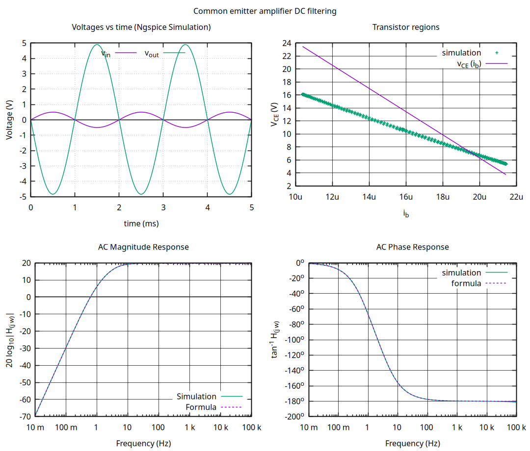
As you can see in bode diagrams gain and phase results are exactly the same, the transistor regions graph diagram difference can be explained because of the load and the coupling capacitor at the output, perhaps the formulation made previously was enough to guarantee the transistor to work in active mode. If you make the load infinitely large you will see how the simulation results approximate to the formula.
In Conclusion
After designing a common emitter amplifier I realized there is one interesting issue that is worth to be mentioned, which is the high output resistance this kind of amplifier has, it clarifies me a lot why buffer amplifiers are needed, without them the gain becomes quite sensible to load changes.
References
If your interested in the simulations made in this post checkout my github repo.
I used the following books as reference material, I strongly recommend the second, it is a great learning resource.