Making a charger, the simplest way
If you are familiarized with electronics, you must know that the energy we get from our homes needs to be transformed to make our devices work properly (e.g your Computer, the TV or the Fridge), they are designed to receive a constant amount of current or in other words Direct Current (DC), although the energy provided comes in form of Alternating Current (AC). Today in this blog I will cover the process of passing from AC to DC a fundamental knowledge to design gadgets and electronic devices.
The Theory
To design a circuit we need to define the problem first, so here we go. For an input voltage given by the following equation:
$$ V_{AC} = V_p sin(2 \pi f t) $$
We need to supply a constant voltage $V_{DC}$.
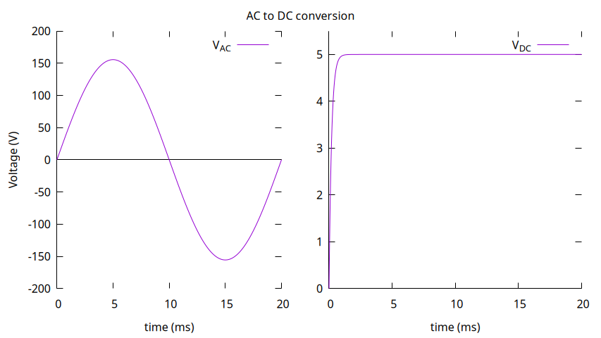
We will set $V_p$ to $110\sqrt{2} V$ and $f$ to $50Hz$, and our desired $V_{DC}$ will be $5V$. The graph below illustrates better what we want:
Here is one solution to the problem, lets see how it works.
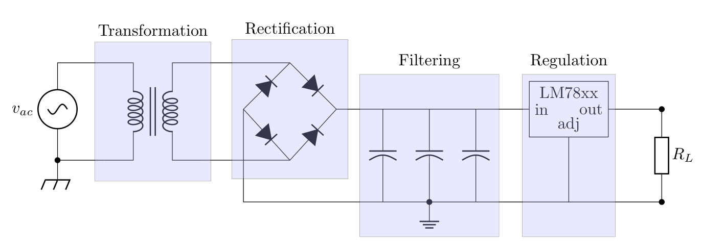
The circuit above is made of four stages:
- Energy Transformation
- Rectification
- Filtering
- Regulation
Energy Transformation
In this stage, the AC voltage ($V_{AC}$) enters a transformer, which converts the high voltage to lower values. This voltage decrease is compensated by an increase in current, hence the name “transformer”. The primary function of a transformer is to alter how energy manifests itself, and in our case, we are transforming electric potential energy (manifested as voltage) into magnetic energy (manifested as current).
Rectification
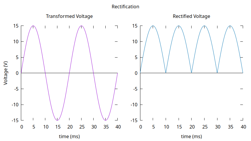
Once the voltage is transformed to lower values the next step is to rectify it, which basically means trying to obtain the positive phases of the transformed voltage. In the previous image on rectification step there is a circuit known as the diode bridge; this arrangement only allows the current to flow in one direction, consequently its output voltage will only be positive even in the negative phases of the bridge diode input. In the graph below you can see the result of connecting the transformed voltage to an ideal diode bridge.
Filtering
After the rectification stage, we have a positive voltage signal increasing and decreasing at a certain frequency, so why not to use capacitors to compensate voltage reduction cycles, in fact they will prevent fast voltage changes acting as Frequency Filters making the voltage signal look more like a constant voltage source as you can see in the graph below (a spoiler of the simulation results) where $V_F$ corresponds to the filtered voltage.
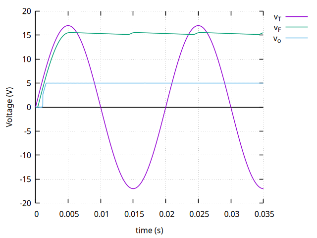
Notice how $V_F$ looks almost like a DC signal but with ripples.
Regulation
Now that the voltage is filtered, we can regulate it to the value we want (5V), this can be achieved using a circuit known as the voltage regulator, they come in two flavors, linear and switched, for the sake of simplicity we will stick with linear voltage regulators, and will cover the setup for the switched ones in a later post.
The basic principle behind its working lies in the following scheme:
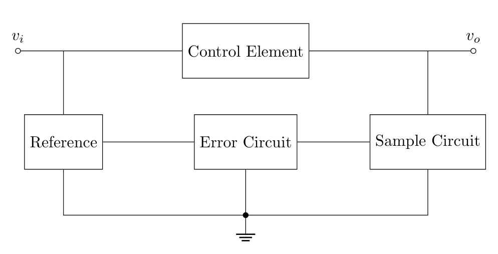
And below there is a basic implementation:
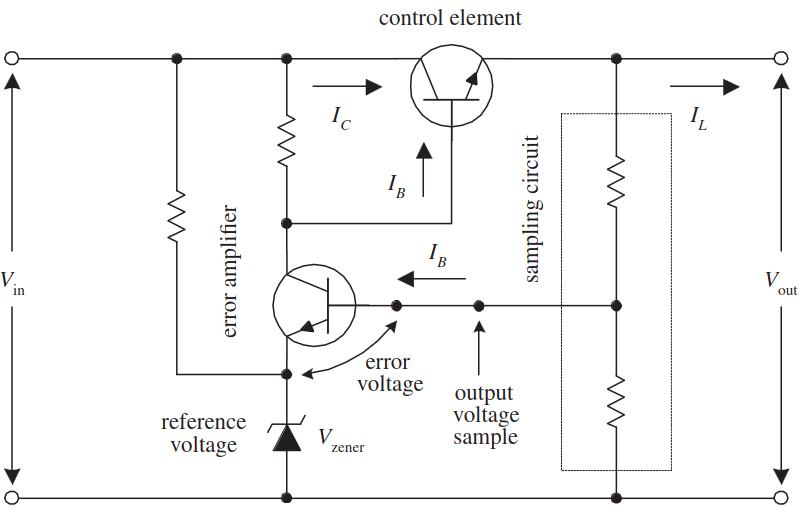
From the scheme above the regulator monitors the voltage through the sampling circuit (in this case the voltage divider), which feeds the amplifier or better called the error circuit that uses as reference the voltage on the Zener diode, finally the error amplifier output fed the control circuit (the transistor on the top) to control the load current (R_L in our scheme above).
Devices available in the market are more complex than the explained above but at their core all linear regulators follow the same principle.
Compared with switched voltage regulators, linear voltage regulators efficiency is usually worse, that’s the reason we don’t see them too often on cellphone or computer chargers, however they are a good starting point to make AC-DC converters.
The simulation
Once you grasped on the details of the circuit, it is time to make a simulation and see if it works, we will use Ngspice, the de facto open source simulation software for electronic and electric circuits, it is the back-end for various graphic an non graphical software applications which require circuit simulation, you can take a look here to check if your EDA is using it behind the scenes, we will stick with vanilla command line Ngspice in this blog post.
Before starting, let me redraw the same circuit with the nodes labeled to ease the process of representing the circuit.

Now lets code for representing the circuit:
 1AC-DC Linear Regulator
 2
 3.inc ./lib/generic.lib
 4.inc ./lib/regulators.lib
 5
 6* Transformation
 7Vac ~1 ~2 sin(0 155.6 50)
 8Xt ~1 ~2 acs1 acs2 TRANSFORMER Lout=1.19
 9
10* Rectification
11Xr acs1 acs2 in gnd RECTIFIER
12
13* Filtering
14C1 in gnd 100u
15C2 in gnd 100u
16C3 in gnd 10u
17
18* Regulation
19Xrv in gnd out LM7805
20Rl out gnd 1k
21
22.control
23set filetype ascii
24tran 100us 35ms
25wrdata results/voltages.raw v(acs1,acs2) v(in) v(out)
26shell gnuplot ac2dc_linear.gnuplot
27.endc
28.end
In Ngspice every circuit is defined by its components and how they are connected, for instance check out line 7 it is telling Ngspice to put a sine voltage source within the nodes ~1 and ~2.
7Vac ~1 ~2 sin(0 155.6 50)
If the first word of a line starts with an alphabetic character it will represent an electronic component of the circuit, the character in itself represents the device type you want to simulate, below you can see a list of some characters and what devices they represent.
- C: stands for Capacitor
- D: stands for Diode
- V: stands for Voltage source
- R: stands for Resistor
- L: stands for Inductor
- X: stands for a custom sub-circuit device
The other characters on the first word’s line identify the device.
After defining the device type the subsequent arguments indicate Ngspice which
nodes are connected to the device, the number of arguments vary depending of
how many nodes are required for the device, to have a better idea check line 8
where the device Xt needs the nodes ~1, ~2, acs1 acs2 to work
properly.
8Xt ~1 ~2 acs1 acs2 TRANSFORMER Lout=1.19
Once the device type and its nodes are defined, you have to set its properties
using the remaining arguments, like lines 14 to 16 where we set C1, C2 and
C3 capacitances to be 100uF, 100uF and 10uF respectively.
14C1 in gnd 100u
15C2 in gnd 100u
16C3 in gnd 10u
Great, we can now describe any circuit made of Resistors, Diodes, Inductors and
more but, What do the words TRANSFORMER, RECTIFIER and LM7805 mean?, what
properties are needed to make X components work? Why the code above does not
run?. Well the answer to those questions reside on lines 3 and 4:
3.inc ./lib/generic.lib
4.inc ./lib/regulators.lib
They tell Ngspice to include the files ./lib/generic.lib
and ./lib/regulators.lib. If the first character of a
line starts by . its first word will be interpreted as a command, in this case
.inc includes an external file with more Ngspice code. Lets see
./lib/generic.lib contents:
 1.subckt TRANSFORMER in1 in2 out1 out2 Lin=100 Lout=100 R1=1m R2=1m
 2* in1 .---x  x---. out1
 3*         )||(
 4*         )||(
 5* in2 .---x  x---. out2
 6
 7* Inductances
 8Lin in1 intin {Lin}
 9Lout out1 intout {Lout}
10
11* Resistances
12R1 intin in2 {R1}
13R2 intout out2 {R2}
14
15* Coupled Factor
16K1 Lin Lout 1
17
18.ends TRANSFORMER
19
20.subckt RECTIFIER ac1 ac2 out gnd
21D1 ac1 out DI_ABS10A
22D2 ac2 out DI_ABS10A
23D3 gnd ac2 DI_ABS10A
24D4 gnd ac1 DI_ABS10A
25.MODEL DI_ABS10A D  ( IS=3.47n RS=42.6m BV=1000 IBV=5.00u
26+ CJO=25.2p  M=0.333 N=1.70 TT=4.32u )
27.ends RECTIFIER
Take a look at lines 1 and 18 and also lines 20 and 27, the commands .subctk
and .ends are the block statements to create a custom circuit in Ngspice.
Here its a simplified version of .subctk .ends structure:
1.subctk LABEL node1 node2... parameter1=value parameter2=value...
2* In ngspice every line starting with '*' is a comment
3
4* Ngspice code
5
6.end LABEL
As you can see above, .subctk directive must be followed by a label, its nodes
and its custom parameters. To use a parameter value within the .subckt block
enclose the identifier between curly brackets like lines 8, 9, 12 and 13 where
Lin, Lout, R1 and R2 parameter values are used to define the components
with the same name.
 7* Resistances
 8Lin in1 intin {Lin}
 9Lout out1 intout {Lout}
10
11* Resistances
12R1 intin in2 {R1}
13R2 intout out2 {R2}
Finally we have the mysterious .model directive at line 25, and also 26, I
forgot to mention that every line starting with a + character is interpreted
as part of the previous line:
25.MODEL DI_ABS10A D  ( IS=3.47n RS=42.6m BV=1000 IBV=5.00u
26+ CJO=25.2p  M=0.333 N=1.70 TT=4.32u )
It basically is like and alias to set the properties of a builtin device which
is pretty knee on devices that require setting a considerable amount of
parameters (like diodes or transistors), for instance D1, D2, D3 and D4
properties were configured using the model definition given in line 25 which is
structured in the following way:
.model mname type(pname1=pval1 pname2=pval2 ... )
Where mname is the label to identify the model and type corresponds to any
of the builtin device types defined in Ngspice, depending of the device you must
look the Ngspice manual
to set the proper parameters in order to simulate the device you want.
The circuit is already defined and we finally understand what does each component, now lets configure the simulation in itself, that’s the purpose of lines 22 to 27 on the circuit file (the first one).
22.control
23set filetype ascii
24tran 100us 35ms
25wrdata results/voltages.raw v(acs1,acs2) v(in) v(out)
26shell gnuplot ac2dc_linear.gnuplot
27.endc
With the exception of comments inside .control and .endc each line first
word will be treated as a command.
To define the type of simulation we want look at line 24 it tells Ngspice to make transient simulation, the first argument sets the time step ($100 \mu s$) and the second the time to stop the simulation ($35 ms$):
24tran 100us 35ms
In line 25 the command wrdata saves the results which in our case are the
transformed ($V_T$), filtered ($V_F$) and regulated $(V_o)$ voltages, which are
referenced by using the keyword v and the specifying the nodes we want in
parenthesis, see the line 25 to understand how to reference them.
25wrdata results/voltages.raw v(acs1,acs2) v(in) v(out)
By default wrdata saves the output in binary form, however with the directive
set filetype ascii on line 22 Ngspice saves the data results as space
separated columns where each pair of them will correspond to time and voltage
values of the simulation, below you can see how it looks like.
 0.00e+00  3.74e-45  0.00e+00  3.31e-33  0.00e+00  7.06e-43
 1.00e-06  5.33e-03  1.00e-06  1.34e-17  1.00e-06  1.49e-20
 1.08e-06  5.78e-03  1.08e-06  1.01e-13  1.08e-06  1.15e-15
 1.25e-06  6.67e-03  1.25e-06  3.30e-13  1.25e-06  1.70e-15
 1.58e-06  8.46e-03  1.58e-06  8.93e-13  1.58e-06  2.04e-15
 2.26e-06  1.20e-02  2.26e-06  2.46e-12  2.26e-06  3.17e-15
 3.60e-06  1.92e-02  3.60e-06  7.52e-12  3.60e-06  5.28e-15
 ...
The statement shell gnuplot ac2dc_linear.gnuplot is just an external bash
command called to plot the results saved on results/voltages.raw, if you are
curious about how it works take a look at the gnuplot file in this
repo.
Now that you understand how to make the simulation we can finally run the program using the following command:
$ ngspice -b ac2dc.cir
Here are the results:

In conclusion
AC to DC conversion is a fundamental concept in the design of lots of circuits, in its simplest implementation the voltage needs to pass through four stages, energy transformation, voltage rectification, voltage filtering and finally voltage regulation.
In this blog we learned the purpose of each stage and how to simulate them all to understand an AC-DC converter, it is now up to you to create the implementation, if you need an example checkout the following link it is a dummy implementation made in Kicad which might be pretty useful to make your own circuit.